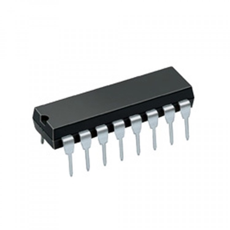


TL494 Power Inverter IC
The TL494 IC is a fixed frequency current-mode PWM controller IC with all the functions that are required in the construction of the pulse-width modulation (PWM) control circuit on a single chip.
TL3843 Pinout Configuration
Pin Number | Pin Name | Description |
1 | 1IN+ | Noninverting input to error amplifier 1 |
2 | 1IN- | Inverting input to error amplifier 1 |
3 | FEEDBACK | Input pin for feedback |
4 | DTC | Dead-time control comparator input |
5 | CT | Capacitor terminal used to set the oscillator frequency |
6 | RT | Resistor terminal used to set the oscillator frequency |
7 | GND | Ground Pin |
8 | C1 | The collector terminal of BJT output 1 |
9 | E1 | The emitter terminal of BJT output 1 |
10 | E2 | The emitter terminal of BJT output 2 |
11 | C2 | The collector terminal of BJT output 2 |
12 | VCC | Positive Supply |
13 | OUTPUT CTRL | Selects single-ended/parallel output or push-pull operation |
14 | REF | The 5-V reference regulator output |
15 | 2IN- | Inverting input to error amplifier 2 |
16 | 2IN+ | Noninverting input to error amplifier 2 |
TL494 Specifications & Features
- Supply Voltage: 7V to 40V
- Number of Outputs: 2 Output
- Switching Frequency: 300 kHz
- Duty Cycle - Max: 45 %
- Output Voltage: 40 V
- Output Current: 200 mA
- Fall Time: 40 ns
- Rise Time: 100 ns
- Available in 16-pin PDIP, TSSOP, SOIC and SOP Packages
Watch this video it will give you a clear idea about this product.