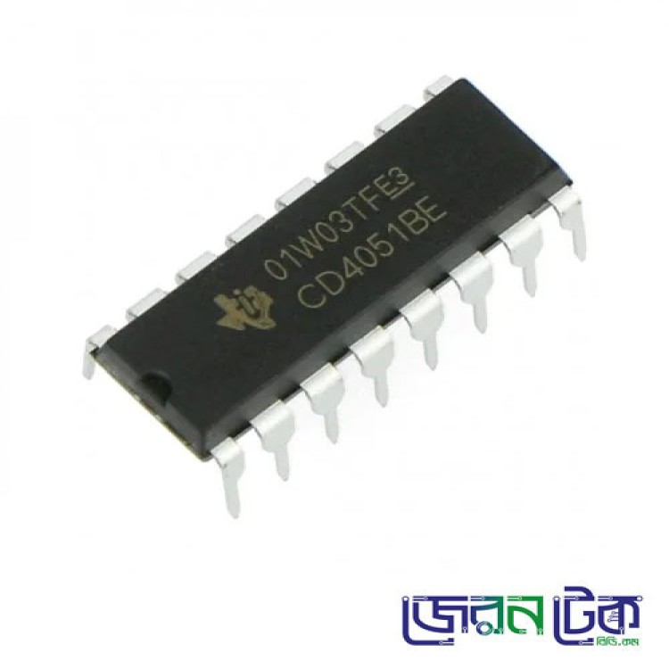


4027 Dual J-K Master/Slave Flip-Flop ic.
CD4027 belongs to the 4000 Series CMOS Logic Family of Integrated Circuits (IC’s) constructed with N- and P-channel enhancement mode transistors. CD4027 has Dual JK Master-Slave Flip-Flop
CD4027 has a supply voltage range of 5V to 20V, which is much higher than any contemporary logic family. It has buffered output which improves transfer characteristics by providing very high gain. All inputs are protected against static discharge with diodes to VDD and VSS.
CD4027 Features
- High-Voltage Types (20V Rating)
- Propagation Delay Time = 60ns (Typ.) at CL = 50pF, VDD = 10V
- Standard Symmetrical Output Characteristics
- 100% Tested for Maximum Quiescent Current at 20V
- 5V, 10V, and 15V Parametric Ratings
- Maximum Input Current of 1μA at 18V Over Full Package Temperature Range; 100nA at 18V and +25oC
- Noise Margin (Over Full Package Temperature Range):
- 1V at VDD = 5V
- 2V at VDD = 10V
- 2.5V at VDD = 15V
CD4027 Specifications
Absolute Maximum Ratings
- DC Supply Voltage Range, (VDD): -0.5V to +20V (Voltage Referenced to VSS Terminals)
- Input Voltage Range, All Inputs: -0.5V to VDD +0.5V
- DC Input Current, Any One Input: ±10mA
- Operating Temperature Range: -55oC to +125oC Package Types D, F, K, H
- Storage Temperature Range (TSTG): -65oC to +150oC
- Lead Temperature (During Soldering): +265oC
- At Distance 1/16 ± 1/32 Inch (1.59mm ± 0.79mm) from case for 10s Maximum
CD4027 Pinout Diagram

CD4027 Pin Description
| Pin No | Pin Name | Description |
| 1 | Q2 | Output Pin 2 |
| 2 | Q2′ | Inverted Output Pin 2 |
| 3 | CLK 2 | Clock Pin 2 |
| 4 | RESET 2 | Reset Pin 2 |
| 5 | K2 | Input Pin K2 |
| 6 | J2 | Input Pin J2 |
| 7 | SET 2 | Set Pin 2 |
| 8 | VSS | Supply Voltage |
| 9 | SET 1 | Set Pin 1 |
| 10 | J1 | Input Pin J1 |
| 11 | K1 | Input Pin K1 |
| 12 | RESET 1 | Reset Pin 1 |
| 13 | CLK 1 | Clock Pin 1 |
| 14 | Q1′ | Inverted Output Pin 1 |
| 15 | Q1 | Output Pin 1 |
| 16 | VDD | Drain Voltage |
4027 Dual J-K Master/Slave Flip-Flop ic.
CD4027 belongs to the 4000 Series CMOS Logic Family of Integrated Circuits (IC’s) constructed with N- and P-channel enhancement mode transistors. CD4027 has Dual JK Master-Slave Flip-Flop
CD4027 has a supply voltage range of 5V to 20V, which is much higher than any contemporary logic family. It has buffered output which improves transfer characteristics by providing very high gain. All inputs are protected against static discharge with diodes to VDD and VSS.
CD4027 Features
- High-Voltage Types (20V Rating)
- Propagation Delay Time = 60ns (Typ.) at CL = 50pF, VDD = 10V
- Standard Symmetrical Output Characteristics
- 100% Tested for Maximum Quiescent Current at 20V
- 5V, 10V, and 15V Parametric Ratings
- Maximum Input Current of 1μA at 18V Over Full Package Temperature Range; 100nA at 18V and +25oC
- Noise Margin (Over Full Package Temperature Range):
- 1V at VDD = 5V
- 2V at VDD = 10V
- 2.5V at VDD = 15V
CD4027 Specifications
Absolute Maximum Ratings
- DC Supply Voltage Range, (VDD): -0.5V to +20V (Voltage Referenced to VSS Terminals)
- Input Voltage Range, All Inputs: -0.5V to VDD +0.5V
- DC Input Current, Any One Input: ±10mA
- Operating Temperature Range: -55oC to +125oC Package Types D, F, K, H
- Storage Temperature Range (TSTG): -65oC to +150oC
- Lead Temperature (During Soldering): +265oC
- At Distance 1/16 ± 1/32 Inch (1.59mm ± 0.79mm) from case for 10s Maximum
CD4027 Pinout Diagram
CD4027 Pin Description
| Pin No | Pin Name | Description |
| 1 | Q2 | Output Pin 2 |
| 2 | Q2′ | Inverted Output Pin 2 |
| 3 | CLK 2 | Clock Pin 2 |
| 4 | RESET 2 | Reset Pin 2 |
| 5 | K2 | Input Pin K2 |
| 6 | J2 | Input Pin J2 |
| 7 | SET 2 | Set Pin 2 |
| 8 | VSS | Supply Voltage |
| 9 | SET 1 | Set Pin 1 |
| 10 | J1 | Input Pin J1 |
| 11 | K1 | Input Pin K1 |
| 12 | RESET 1 | Reset Pin 1 |
| 13 | CLK 1 | Clock Pin 1 |
| 14 | Q1′ | Inverted Output Pin 1 |
| 15 | Q1 | Output Pin 1 |
| 16 | VDD | Drain Voltage |
Watch this video it will give you a clear idea about this product.
Related Product